技術主題: 多裸晶整合晶片之連接線速度檢測與修補技術
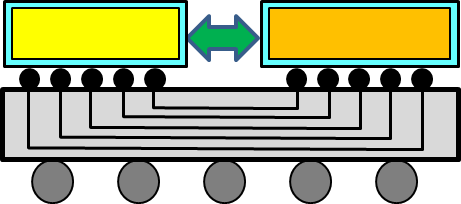
整合多片不同功能的裸晶於單一封裝基座的『三維晶片』技術擁有許多的優點(譬如高接角數,高速、低功耗、小尺寸、支援與高資料通道數的Wide-IO DRAM 的整合等),被普遍認為是未來越來越注重低功耗、異質整合、且輕薄短小的可攜性產品之晶片設計、製造與封裝的主流趨勢。其中,裸晶與裸晶之間的連接線有許多的形式,包括『穿矽連接孔』(Through-Silicon Via),『矽載板中介層』 (Interposer),或是最近新興的晶圓級封裝所採用的『連接線重分配層』(Re-Distribution Layer, RDL) 等。然而,這類的『三維晶片』的設計、測試、與可靠度等各方面仍然存在許多的難題有待克服。
(緣起)
(計畫目標)
我們將以三年的時間進行以下兩個階段的研究:
第一階段【前瞻技術實用化】:先前研發的前瞻技術【連接線速度檢測方法】雖能透過一些低成本的邏輯電路,以了解每一個多裸晶整合晶片中之連接線的傳輸速度,但使用上仍有一些限制(闢如僅能處理兩個端點的連接線等)。為了實用化,我們將持續最佳化這個技術以達成三項擴充功能:(1) 可以處理類似匯流排的多端點的連接線的速度檢測,(2) 可以有效的處理(超過1 千條以上)巨量連接線的晶片,以支援與 Wide-IO DRAM 的整合,(3) 可以處理長度達1 公分的連接線(如晶圓級封裝中『重分配層』連接線)。此外,我們也將擴充【線上連接線修補方法】,使其不需要嵌入式的快閃記憶體的支援就能適用在匯流排的多端點的連接線之自動修補。
第二階段【特製化與最佳化】與【商業化之可行性研究】:我們將製作雛形系統,並與至少兩家以上的公司合作,一方面特製化與最佳化我們解決方案的使用者介面,另一方面透過與這些公司的實作,了解這些技術的真正價值,以利商品化的可行性評估。
Title: Delay Characterization, Testing, and
Repair for Die-to-Die Interconnects
for Multi-Die Integrated Circuits
3D Integration that includes many dies on a single packaging substrate has been touted as a new trend for future integrated circuits due to its many advantages, such as high-pin count, high-speed, low-power, small form factor, and ability to support the integration with wide-IO DRAM. There could be several different forms of die-to-die interconnects in a 3D-IC, ranging from TSV (Through-Silicon Via), Interposer, to Re-Distribution Layer (RDL) in recently emerging Wafer-Level Processing (WLP) Package. However, to make 3D-ICs feasible and reliable, numerous challenging issues on design, testing, and repair remain to be resolved.
From May 2012, we have been conducting an NPIE (National Project on Intelligent Electronics) project on "Testing and Fault Diagnosis for Interposers in a 3D IC", from which some breakthrough techniques have been developed. In this Academia-Industry Coalition Project, we aim to further explore the values of these previously developed techniques on delay characterization, test, and repair for die-to-die interconnect on multi-die IC through research activities in three aspects, namely, (1) technology improvement for wider adoption, (2) customization and optimization for specific applications, and (3) feasibility study of commercialization.
We will conduct the following research topics in two stages in a time span of three years (Feb. 2015 - Jan. 2018):
Stage 1 on technology improvement: Even though we can characterize the delay of each die-to-die interconnect in a multi-die IC from previously developed techniques, limitations still exist (e.g., it was only suitable for 2-pin interconnects). In order to make our characterization/test method even more practical and useful, we attempt to enhance it by developing an improved version with three new features: (1) It can handle bus-like multi-pin interconnects, (2) It can handle an IC with a large number of interconnects (e.g., one with more than 1000 interconnects) to support integration of wide-IO DRAM, and (3) It can handle extremely long wires that could stretch more than 1cm, which are possible in an RDL used in a (WLP) Package. Also, we will extend our previously developed on-line interconnect repair method to support the self-repair of bus-like interconnects with on-chip flash memory.
Stage 2 on customization, optimization, and feasibility study of commercialization : We will endeavor to cooperate with at least two companies to build a prototype system. Through this process, we will customize our user interface to support different formats for different design/test flows. Also, we will explore the ustomization and optimization for various types of die-to-die interconnects. Furthermore, we assess the real values of our techniques as applied to real industrial applications, and from which we perform the feasibility study of potential commercialization.